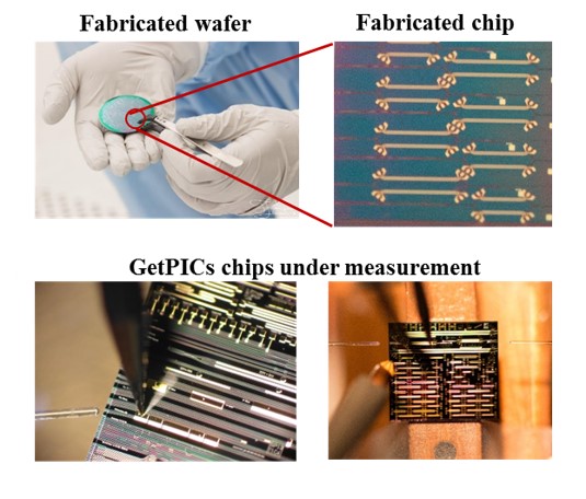
The GetPICs project
The project aims at achieving the improvement of Photonic Integrated Circuit (PIC) building blocks (BBs) for generic integration technology, the design and fabrication of high bit-rate transmitter PICs. Challenges include the introduction of deep UV lithography, semi-insulating (SI)-substrate based technology, SAG (Selective Area Growth) epitaxy techniques, SiBH (Semi-Insulating Buried Hetero-structure) and advanced RF (radio-frequency) circuit engineering. The test vehicles will be validated in transmission systems, and potential markets for the developed PICs will be explored.
Project objectives:
- Demonstration and validation of a fully functional transmitter PIC able to operate at 10x25 Gbps and 4x25 GBauds.
- Implementation and demonstration of buried hetero-structure technology in building complex PICs.
- Technology development and implementation of WDM transmitters in generic technology using selective area growth.
Partners
- III-V Lab, Palaiseau, France (coordinators)
- Eindhoven University of Technology, COBRA research institute, Eindhoven, Netherlands